What is FPGA (Field Programmable Gate Array)? How does it work?

AI (Artificial Intelligence) fundamentally depends on algorithms designed to mimic human cognitive processes, yet the role of hardware is just as critical in this equation. The three primary hardware solutions facilitating AI tasks include field-programmable gate arrays (FPGAs), graphics processing units (GPUs), and central processing units (CPUs). While GPUs and CPUs are widely known, FPGAs often fly under the radar. In this blog post, we'll explore the intricacies of FPGAs and their applications in the tech world.
What is an FPGA?
A Field Programmable Gate Array (FPGA) is a versatile integrated circuit (IC) that can be programmed and reprogrammed by the end user to perform a wide range of functions, unlike the fixed functionalities found in GPUs and CPUs. At its core, an FPGA consists of an array of configurable logic blocks (CLBs), interconnects, and I/O blocks that can be configured to perform various functions. The configuration of the FPGA architecture is generally specified using a language, i.e., HDL (Hardware Description Language), which is similar to the one used for an ASIC (Application Specific Integrated Circuit).
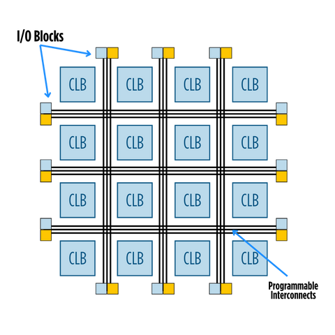
FPGA Architecture
- Configurable Logic Blocks (CLBs): The core of FPGA functionality, these blocks contain logic gates and a small amount of memory that can be programmed to perform various logical functions. They are the building blocks for creating more complex digital circuits.
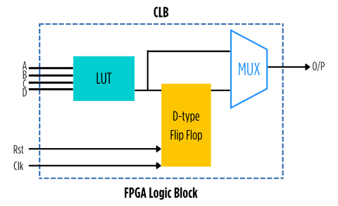
LUT (Look Up Table) implements the combinational logical functions; the MUX (Multiplexer) is used for selection logic, and DFF (D type flip flop) stores the output of the LUT.
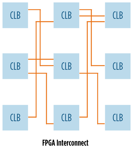
- Programmable Interconnects: A network of programmable wiring that connects the logic blocks. These interconnects can be configured to route signals between different logic blocks, allowing the creation of complex digital circuits by defining how data flows through the FPGA.
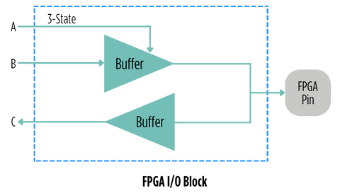
- I/O Blocks (Input/Output Blocks): Located next to every physical input or output pin, these blocks connect the internal logic of the FPGA to the external environment. They can be programmed to act as inputs, outputs or tri-states, enabling the FPGA to communicate with external devices and systems.
Types of FPGAs
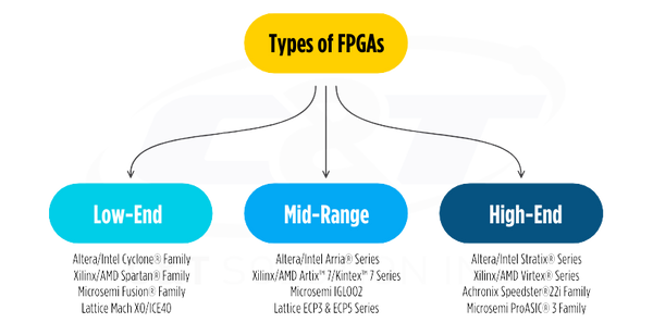
- Low-End FPGAs: developed for low power consumption, low logic density, and low complexity per chip. Examples of low-end FPGAs are the Cyclone family from Altera, the Spartan family from Xilinx, the Fusion family from Microsemi, and the Mach XO/ICE40 from Lattice Semiconductor.
- Mid-Range FPGAs: developed to balance performance and cost. Examples of Mid-range FPGAs are Arria from Altera, Artix-7/Kintex-7 series from Xlinix, IGL002 from Microsemi, and ECP3 and ECP5 series from Lattice semiconductor.
- High-End FPGAs: developed for logic density and high performance. Examples of High-end FPGAs are the Stratix family from Altera, the Virtex family from Xilinx, the Speedster 22i family from Achronix, and the ProASIC3 family from Microsemi.
Advantages of FPGAs
- Flexibility: FPGAs can be reprogrammed to perform different tasks or update the functionality of a device after it has been deployed. This allows for modifications and improvements without needing to redesign the hardware.
- Rapid Prototyping: Designers can quickly implement and test their designs on FPGAs, making them ideal for prototyping and iterative development processes.
- Lower Initial Costs: For low to medium-volume productions, FPGAs generally have lower upfront costs compared to developing an ASIC, as there are no expensive fabrication costs involved.
- Shorter Time to Market: Since FPGAs do not require a manufacturing process after design, they can significantly reduce the time to market for new devices.
FPGA Applications
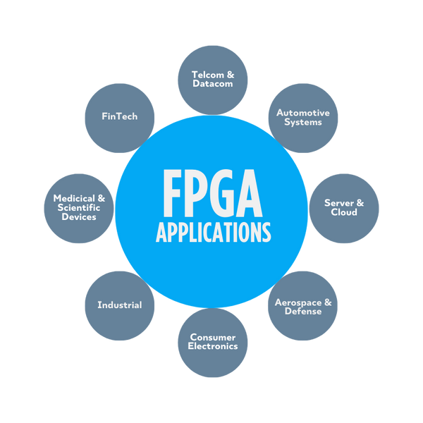
- Telecommunications: FPGAs are essential for signal processing and updating network protocols without replacing hardware.
- Automotive Systems: Used in driver assistance, infotainment, and V2X communications, FPGAs allow post-sale updates.
- Data Centers: Accelerate data processing, encryption, and network management, enhancing server efficiency.
- Aerospace and Defense: FPGAs provide reliability in harsh environments, handling radar, communications, and encryption.
- Consumer Electronics: Utilized for processing in cameras, TVs, and home systems, improving digital experiences.
- Industrial Control: Streamline control systems, automation, and machine vision, facilitating real-time processing.
- Medical & Scientific Instruments: Essential in imaging equipment, FPGAs process complex algorithms quickly, ensuring rapid diagnostics. Support research with precision and speed in data acquisition and analysis.
- Financial Technology: Enable faster high-frequency trading with low-latency, high-throughput processing capabilities.
- Artificial Intelligence and Machine Learning: Accelerate AI/ML training and inference, supporting rapid development and deployment.
What is the difference between FPGAs and ASICs?
While FPGAs are types of integrated circuits with programmable hardware fabric, ASICs, or Application-Specific Integrated Circuits, are types of semiconductor chips designed for a specific application or purpose rather than intended for general-purpose use. ASICs are hardwired to execute specific functions and cannot be reprogrammed or repurposed once manufactured. Here is a closer comparison between the two:
| Feature | FPGA | ASIC |
|---|---|---|
| Flexibility | High (reprogrammable) | Low (not reprogrammable) |
| Performance | Lower than ASIC | Higher Performance for specific tasks |
| Power Consumption | Higher compared to ASIC | Lower (optimized for efficiency) |
| Development Cost | Low (no NRE cost) | High (high NRE cost) |
| Production Cost per Unit | Higher compared to ASIC | Lower (optimized for volume) |
| Time to Market | Shorter (reprogrammable, adaptable) | Longer (due to design and fabrication) |
| Reprogrammability | Yes (can change algorithms post-production) | No (fixed design) |
| Suitable Production Cycle | Small to medium scale | High volume (to offset NRE costs) |
| Design Cycle | Shorter | Longer |
In summary, the choice between FPGA and ASIC depends on the specific application requirements. FPGAs are favored for their adaptability and quick deployment, ideal for evolving environments, prototyping, and medium-scale productions requiring flexibility. Conversely, ASICs excel in efficiency, offering optimized performance and lower power consumption, making them the better choice for high-volume, stable applications where the high initial cost can be offset by large-scale production benefits. The decision between using an FPGA or an ASIC ultimately depends on factors such as required flexibility, performance needs, power consumption, and production volume.

